In high-performance computing, clock speed (GHz) is only half the story. The real bottleneck in modern systems is the “Movement of Data.” At MasterWebTool.com, we analyze the Bus Architecture—the high-speed highway system that allows a CPU to communicate with RAM and GPUs at speeds exceeding 128 GB/s.
1. What is a “Bus” in 2026 Computing?
A Bus is a physical communication interface consisting of conductive traces on a PCB or silicon die.
The Fact: Modern high-end CPUs like the Intel Core i9-14900K or AMD Ryzen 9 7950X use internal buses that operate at the frequency of the CPU cores (up to 6.0 GHz).
The Bandwidth Formula: Bandwidth is calculated as:
$$Bandwidth = \text{Bus Width (bits)} \times \text{Clock Speed (Hz)} / 8$$
🔗 Related Article: Before data travels, the “Engine” (CPU) must be built. Learn about 3nm and 5nm chip manufacturing in our guide: What Are Semiconductor Chips and How Do They Work?
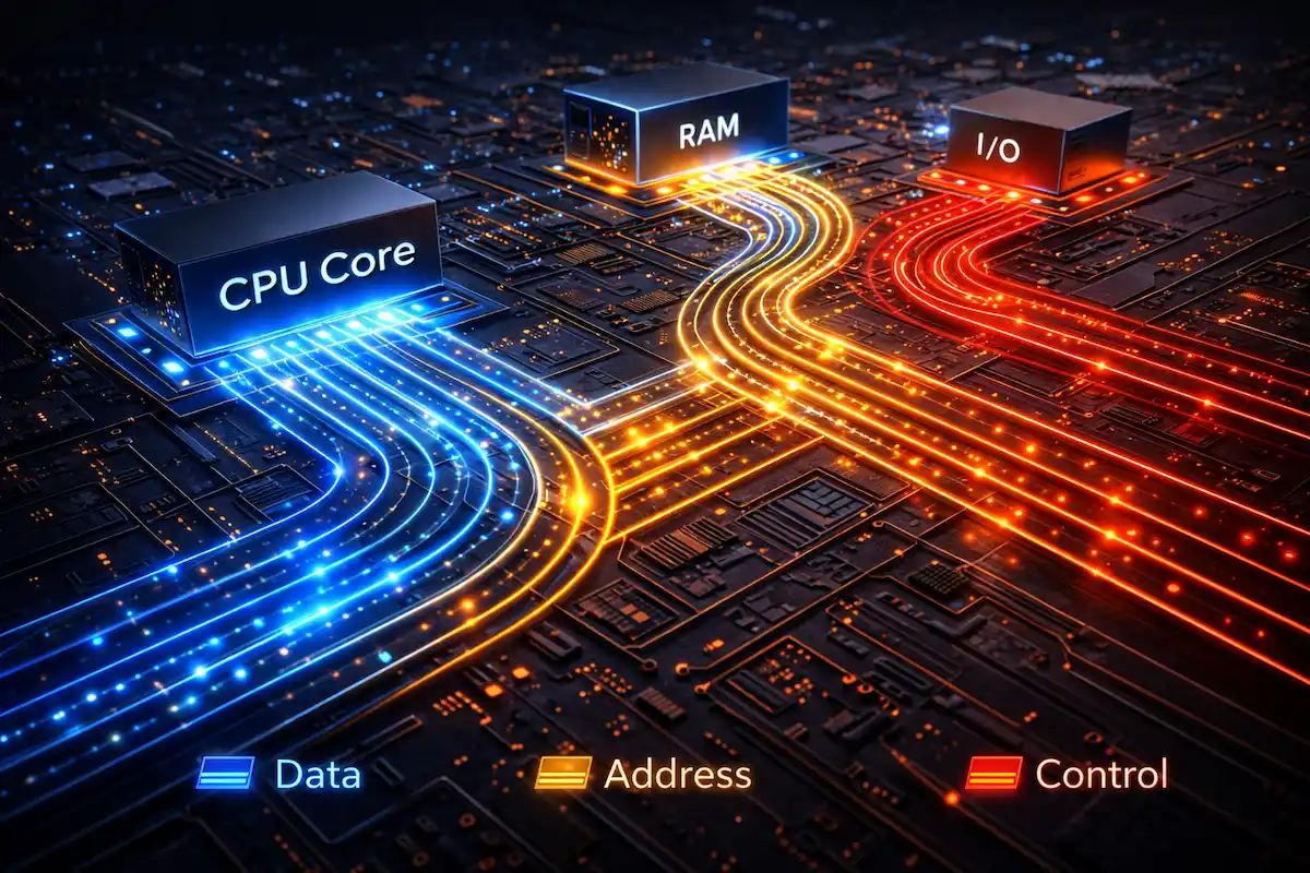
2. The Trinity of System Buses (Technical Data)
The system architecture relies on three specific types of buses to manage information flow:
A. The Data Bus (The Payload)
This carries the actual bits.
The Fact: Most modern consumer CPUs use a 64-bit Data Bus. This means in one single clock cycle, the CPU can move 64 bits (8 bytes) of data.
Calculation: At a 3.2 GHz memory clock, a 64-bit bus provides a theoretical peak of 25.6 GB/s per channel.
B. The Address Bus (Memory Limits)
This determines how much memory the CPU can “address” or recognize.
32-bit Limit: $2^{32} = 4,294,967,296$ bytes (4 GB limit).
64-bit Reality: Modern 64-bit address buses can theoretically address 16 Exabytes of RAM, though physical motherboards currently cap this at 128GB to 2TB.
C. The Control Bus (The Command Center)
It handles synchronization signals. If you are using an Image Compressor, the Control Bus sends “Interrupt” signals to the CPU to prioritize the compression task over background processes.
3. The Shift from Parallel to Serial: PCIe Gen 5 & 6
Historically, we used Parallel Buses (PATA/IDE). Today, we use Serial Buses (PCIe) because parallel wires suffer from “Skew”—where bits arrive at different times due to tiny physical length differences in the wires.
| Bus Standard | Lane Speed (per lane) | Max Bandwidth (x16 slot) |
| PCIe 4.0 | 16 GT/s | 64 GB/s |
| PCIe 5.0 | 32 GT/s | 128 GB/s |
| PCIe 6.0 (Latest) | 64 GT/s | 256 GB/s |
🔬 Tech Insight: Moving data at 256 GB/s generates extreme heat, requiring advanced cooling and power efficiency. See how GaN technology is solving this: Silicon vs. Gallium Nitride (GaN): The Future of Power Chips.
4. Northbridge and Southbridge: The Legacy vs. Modern SOC
Old motherboards had a “Northbridge” chip to handle high-speed traffic (RAM/GPU) and a “Southbridge” for slow traffic (USB/SATA).
Modern Fact: In 2026, these are integrated into the CPU itself (System on a Chip – SoC). This reduces the physical distance data travels, cutting “Latency” (delay) from 100ns down to <10ns.
5. Why Does This Matter for Web Performance?
High-speed Bus Architecture is the reason why MasterWebTool can process complex JavaScript and large images instantly.
Memory Bottlenecks: Even with a fast CPU, a slow bus (like an old PCIe 3.0 slot) will throttle a modern NVMe SSD, making your tools feel sluggish.
Optimization: When we build tools, we optimize for “Cache Locality,” ensuring the Data Bus spends less time fetching from slow RAM and more time in the lightning-fast L3 Cache.
Frequently Asked Questions (FAQ) – Bus Architecture
Q1. What is the difference between a 32-bit and a 64-bit Address Bus?
The width of the address bus determines the maximum amount of RAM the CPU can access. A 32-bit bus is limited to 4 GB ($2^{32}$ addresses), whereas a 64-bit bus can theoretically address up to 16 Exabytes ($2^{64}$ addresses). This is why modern high-performance PCs require a 64-bit architecture to use 8GB, 16GB, or more RAM.
Q2. Why did the industry move from Parallel to Serial Buses (like PCIe)?
In the past, parallel buses (like PATA) sent multiple bits at once. However, as speeds increased, “Clock Skew” occurred—where bits arrived at different times due to tiny physical variations in wire length. Serial Buses (PCIe) send data one bit at a time but at incredible frequencies (GigaHertz), eliminating interference and providing much higher bandwidth (up to 256 GB/s in PCIe 6.0).
Q3. Can a slow Bus Architecture bottleneck a fast CPU?
Absolutely. If you have a high-end CPU (like a Ryzen 9) but your motherboard only supports an older bus standard (like PCIe 3.0), your high-speed NVMe SSD or GPU will be “throttled.” The CPU will spend idle cycles waiting for data to travel across the slow “highway,” reducing overall system efficiency.
Q4. What is the role of the Control Bus in multitasking?
The Control Bus acts as the “Traffic Police.” When you are running multiple tools on MasterWebTool.com, the Control Bus manages “Interrupt” signals. It tells the memory and I/O devices when to “Read” or “Write” and ensures that data packets don’t collide on the Data Bus.
Q5. How does Bus Architecture affect Web Page Load Speed?
For developers, bus architecture is the backbone of local processing. When a browser executes heavy JavaScript or uses an Image Compressor, the speed at which data moves between the CPU Cache, RAM, and the SSD (via the System Bus) directly determines how fast the tool responds to the user.
6. Conclusion: The Invisible Infrastructure
Without the evolution of Bus Architecture—from the 8-bit ISA buses of the 1980s to the 256GB/s PCIe 6.0 highways of today—the AI revolution would be impossible. These “Silicon Highways” are the unsung heroes of the digital age.
🛠️ Related MasterWebTool Resources
FIRE Calculator – Plan your retirement with high-speed precision.
Image Compressor – Use the power of optimized bus architecture to speed up your site.
Inflation Calculator – Protect your wealth against the rising cost of server-grade hardware.


