As India targets a $10 Billion Semiconductor Mission, understanding the “Brain” of every electronic device—the Silicon Chip—has never been more critical. From theIndia AI Impact Summit 2026to the rise of domestic “Fabs,” the semiconductor manufacturing process is the backbone of our digital sovereignty.
At MasterWebTool, we break down this ultra-complex engineering marvel into a simplified, step-by-step roadmap that explains how sand turns into supercomputers.
The AI Link: High-performance AI models require advanced GPUs built on 3nm and 5nm nodes.
India’s Role: With massive investments in Dholera and Sanand, India is becoming a global chip-making hub.
Economic Impact: The sector is projected to create over 1 million high-tech jobs by 2030.
1. What is Semiconductor Manufacturing? (Explained)
Semiconductor manufacturing, often called “Fabrication” or “Fab,” is the process of creating integrated circuits (ICs) on a thin slice of silicon. This is done at a Nanometer (nm) scale—where a single transistor is thousands of times smaller than a human hair.
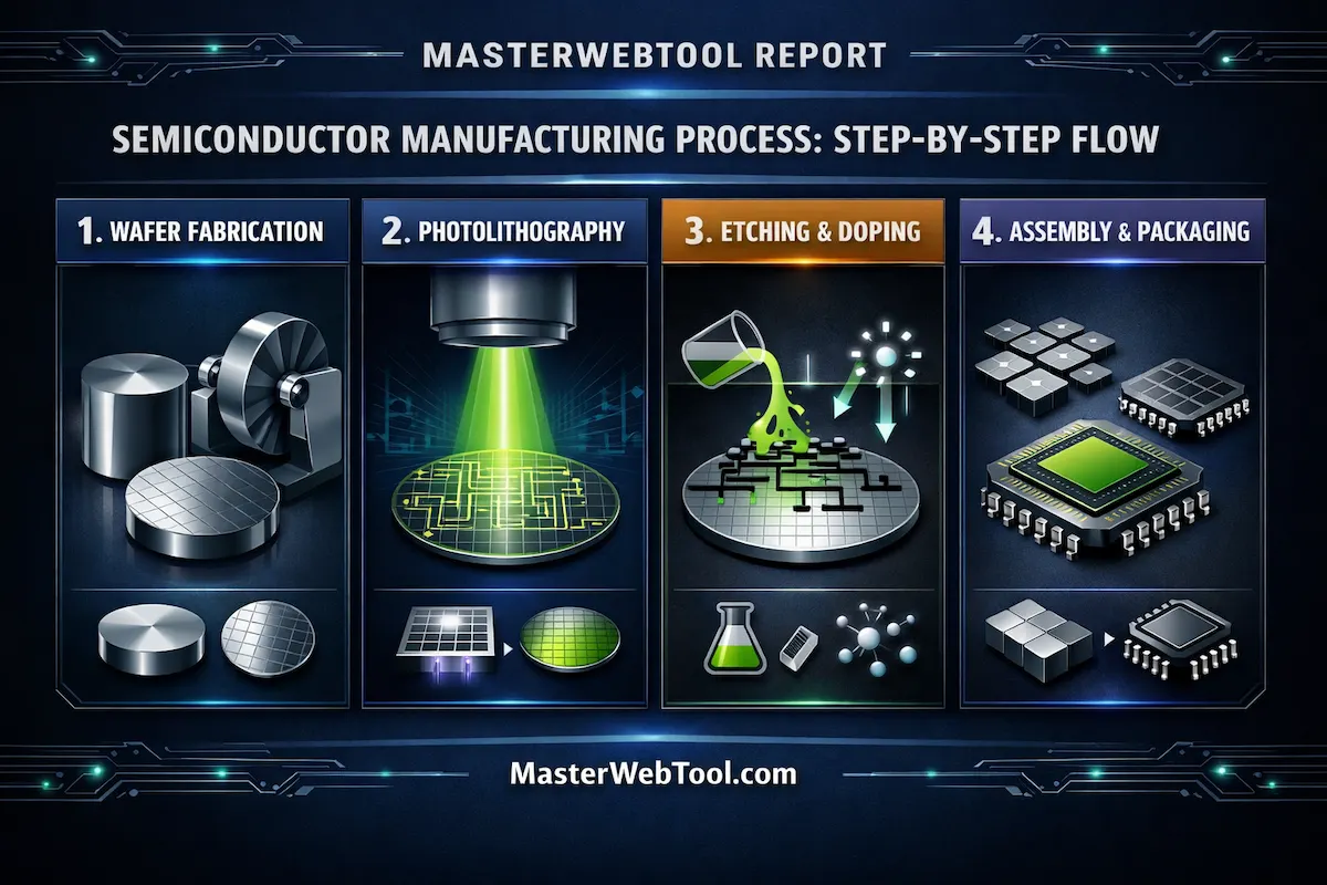
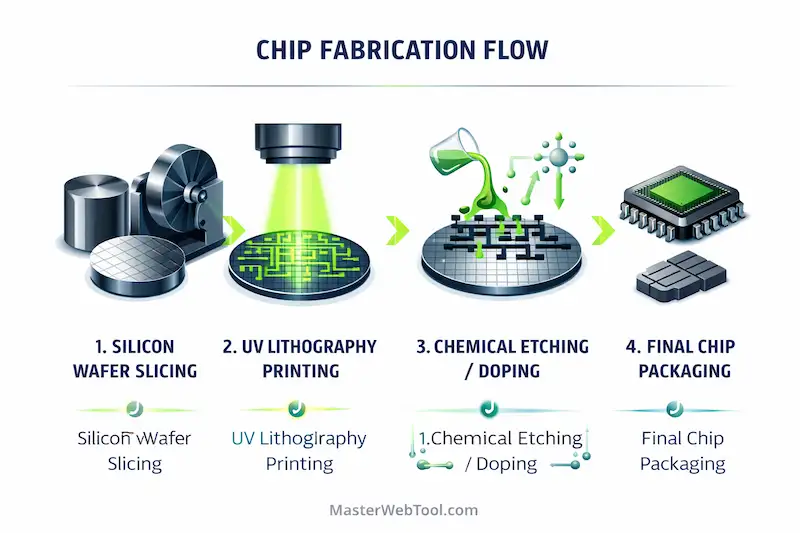
Google users often search for a “Flow Chart” or “Steps” to understand this complex cycle. Below is the simplified flow of how a chip is born.
Step-by-Step Flow: Understanding the sequential journey of silicon from raw material to final chip packaging.
(Alt Text: Horizontal flow chart showing semiconductor manufacturing steps from wafer to chip for MasterWebTool)
The 4 Core Stages of Chip Fabrication
Stage
Process Name
Key Action
Stage 1
Wafer Fab
Slicing pure Silicon ingots into ultra-thin, polished wafers.
Stage 2
Photolithography
Using EUV (Extreme Ultraviolet) light to “print” circuit designs.
Stage 3
Etching & Doping
Removing excess material and injecting ions to create transistors.
Stage 4
Packaging
Dicing the wafer into individual chips and sealing them in protective cases.
3. Essential Tools for Semiconductor Analysis
If you are looking for a course or PPT level understanding, these free tools and resources are industry-standard:
WikiChip: The ultimate digital library to compare chip architectures and transistor density.
EDA Playground: A web-based tool to practice Verilog/VHDL—the language used to design chip logic before it hits the factory.
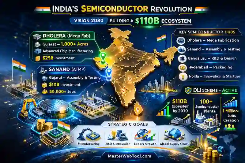
4. India’s Strategic Position in the Global Chip Race
🇮🇳 The Hub of Innovation: From Gujarat’s Mega Fabs to Bengaluru’s R&D, India is building a complete $110B semiconductor ecosystem by 2030.
The India AI Impact Summit 2026 highlighted that without domestic chips, “Sovereign AI” is impossible. India’s focus on Design-Linked Incentives (DLI) is attracting global giants like Micron and Tata Electronics to build a local ecosystem.
Dholera Mega-Fab: Currently building capacity for 28nm and 40nm nodes.
Tata-PSMC Partnership: Focused on high-volume production for automotive and AI sectors.
5. Challenges: Precision at the Atomic Level
Building a Semiconductor Fab is a massive undertaking because it requires:
Cleanrooms: Environments 1,000 times cleaner than a hospital operation theater.
Ultra-Pure Water: Millions of gallons are needed daily to wash wafers.
Uninterrupted Power: A mere 1-second power fluctuation can ruin an entire batch of chips.
Frequently Asked Questions (FAQs)
Q1. What are the 7 main steps of semiconductor manufacturing?
The 7 steps are: Cleaning, Deposition, Photolithography, Etching, Doping, Metallization, and Testing/Packaging.
Q2. Why is silicon used for chips?
Silicon is an ideal semiconductor because it is abundant (found in sand) and its electrical conductivity can be precisely controlled.
Q3. How long does it take to make a single chip?
The entire process from a raw wafer to a finished processor can take 3 to 4 months, depending on the complexity of the design.
Conclusion: Securing India’s Digital Future
Semiconductor manufacturing is no longer just an industrial process; it is a geopolitical necessity. By mastering the “Fab,” India is securing its future in AI, 6G Telecommunications, and Space exploration.