In the modern era, silicon chips are the “silicon soul” of every digital device. From the smartphone in your pocket to the advanced AI servers discussed at the India AI Impact Summit 2026, these microscopic marvels power our world. But how does a grain of sand transform into a trillion-transistor processor?
In this comprehensive 1500-word guide,MasterWebTooltakes you inside the multi-billion dollar “Cleanrooms” to explain the atomic-level engineering of silicon chips.
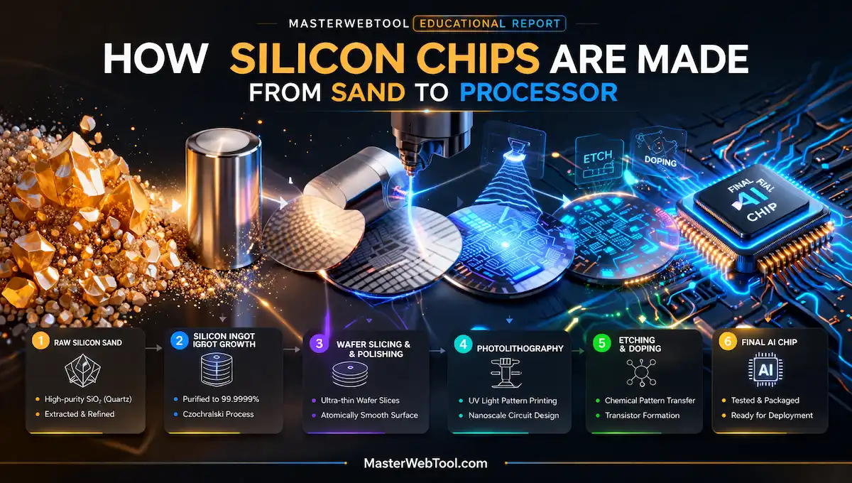
1. The Raw Material: From Sand to Solar Grade Silicon
It all begins with Quartz Sand (Silicon Dioxide). Silicon is the second most abundant element on Earth, but for chip-making, it needs to be “Electronic Grade” (99.9999999% pure).
The Purification Process
The sand is melted in massive electric arc furnaces at temperatures exceeding 1900°C. Through a chemical process called the Siemens Process, it is refined into Polysilicon. This material is then melted again to grow a single, massive crystal known as an Ingot.
The Czochralski (CZ) Method
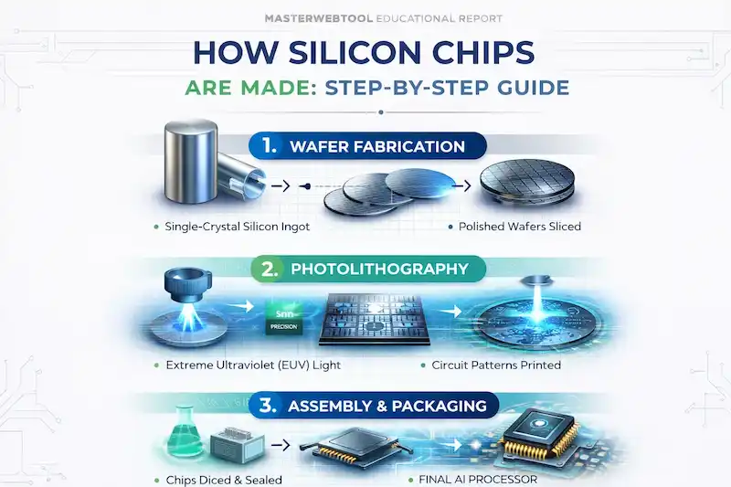
A small “seed crystal” is dipped into molten silicon and slowly rotated and pulled upward. This creates a solid, cylindrical crystal ingot weighing up to 100kg.
Once the Ingot is ready, it is sliced into paper-thin discs using a high-precision diamond saw. These discs are called Wafers.
Lapping and Polishing
A raw wafer is rough. To make it ready for circuits, it undergoes Chemical Mechanical Planarization (CMP). This process polishes the wafer until it is flatter than any other surface on Earth—perfectly mirror-like at an atomic level.
3. Photolithography: Printing the Microscopic Design
From Wafer to Final Chip: A sequential breakdown of the 3 main phases of semiconductor creation.
This is the most expensive and complex part of the process. If you want to understand How Silicon Chips Are Made, you must understand Photolithography.
The Photoresist Coating
The wafer is coated with a light-sensitive liquid called Photoresist. It spins at high speeds to ensure a perfectly even layer.
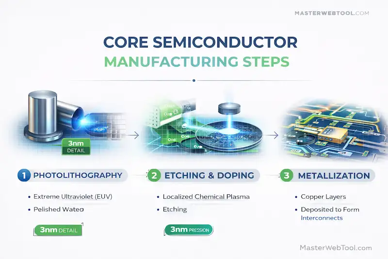
Extreme Ultraviolet (EUV) Exposure
Using machines that cost over $150 million each (like those from ASML), EUV light is projected through a “mask” (a stencil of the circuit design). The light “prints” the design onto the photoresist.
💡 Technical Note:This precision is what allowed the industry to move from 14nm to the 3nm and 2nm nodes we see today, a leap forward highlighted in the [India AI Roadmap 2030].
4. Etching and Ion Implantation: Carving the Circuit
After the design is printed, we need to make it permanent.
Chemical Etching
The wafer is doused in chemicals or “plasma gas.” The areas not protected by the photoresist are “etched” away, leaving behind the intricate patterns of the transistors and interconnects.
Ion Implantation (Doping)
Pure silicon is not a good conductor. To make it a “Semiconductor,” we inject it with specific atoms (like Phosphorus or Boron). This process, called Doping, creates the P-type and N-type regions that allow transistors to act as on/off switches.
The Core Process: From printing circuits with EUV light to building microscopic copper interconnects.
5. Deposition and Metallization: Building the Skyscraper
A modern chip isn’t flat; it’s like a 100-story skyscraper built on a microscopic scale.
Chemical Vapor Deposition (CVD)
Thin films of insulating material or conducting metals are “grown” on the wafer surface using gas reactions. This creates the layers of the chip.
The Copper Interconnects
Billions of microscopic copper wires are laid down to connect the millions of transistors. This “wiring” allows signals to travel across the chip at lightning speed.
6. Testing and Sorting: The “Wafer Sort”
Not every chip on a wafer works perfectly. A single speck of dust can ruin a circuit.
The Probing Stage
A machine with needle-thin probes tests every single chip on the wafer. Working chips are marked, and “duds” are discarded.
Quality control at this stage is a major pillar of the India AI Impact Summit 2026] infrastructure goals, ensuring that ‘Made in India’ chips meet global standards.
7. Assembly and Packaging: The Final Armor
The wafer is finally cut into individual pieces using a laser or diamond saw. Each piece is called a Die.
Die Attachment and Wire Bonding
The die is attached to a substrate, and microscopic gold wires connect the chip’s pads to the pins of the package.
Encapsulation
The chip is sealed in a protective ceramic or plastic case. This “Packaging” protects the delicate silicon from heat, moisture, and physical damage.
💡 Fun Fact:India’s first major wins in the semiconductor race are in the ATMP (Assembly, Testing, Marking, and Packaging) sector in Sanand, Gujarat.
8. Why This Process is Critical for India’s Future
As we discussed in our previous deep-dives, semiconductor sovereignty is the key to national security and economic growth. Mastering How Silicon Chips Are Made allows India to:
Reduce Import Dependency: Cutting down the billions spent on importing chips from Taiwan and China.
Power Sovereign AI: Building indigenous LLMs and compute stacks as envisioned in the India AI Roadmap.
Boost High-Tech Jobs: Creating a specialized workforce of over 1 million engineers by 2030.
Frequently Asked Questions (FAQ)
Q1: Why is silicon used for making chips? Silicon is used because it is an “Inherent Semiconductor,” meaning its electrical properties can be easily changed by adding impurities (Doping). It is also very stable at high temperatures.
Q2: What is a Cleanroom? A Cleanroom is a facility where the air is filtered to be 10,000 times cleaner than a hospital. Even a single skin cell or dust particle can destroy a 3nm chip during the photolithography stage.
Q3: How long does the entire process take? From raw wafer to a finished, packaged chip, the process can take 12 to 16 weeks. It is the most time-consuming manufacturing process in the world.
Conclusion: The Silicon Century
The journey of a chip—from sand to a trillion-transistor processor—is a testament to human ingenuity. As India builds its own “Fabs” and ATMP plants, understanding this process helps us appreciate the complexity behind every click, tap, and AI prompt.