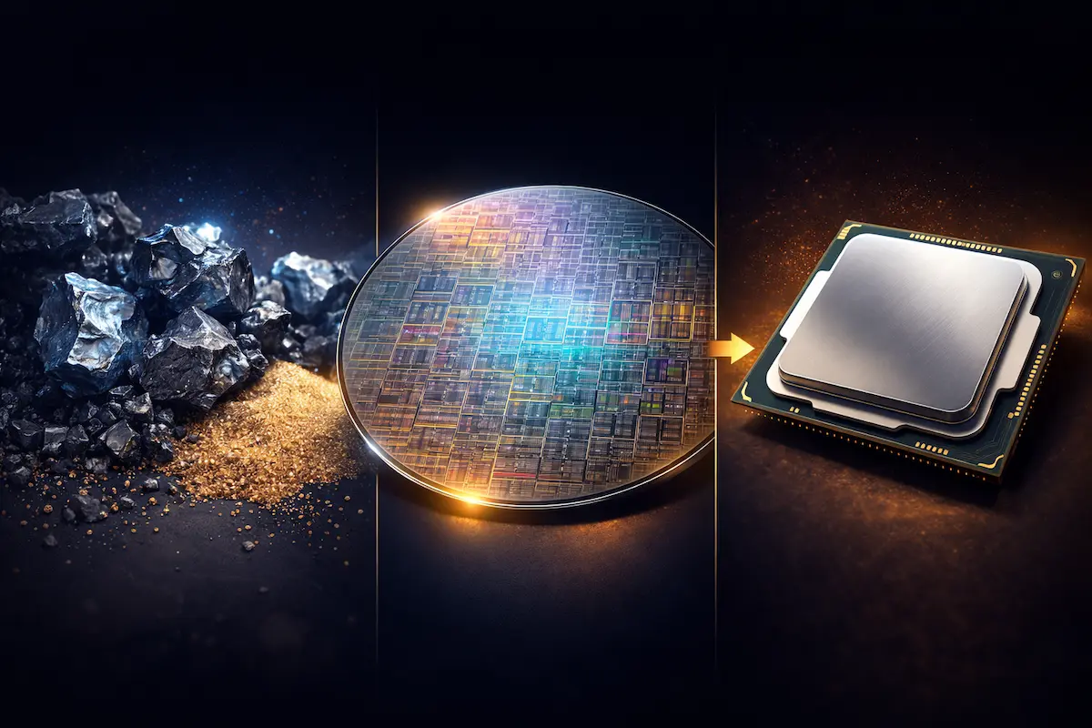
Take a moment to look at the device you are using right now—whether it is a smartphone, a sleek laptop, or a desktop computer. At the heart of this machine lies a microscopic marvel of human engineering: the microchip. But have you ever wondered how a simple grain of sand is transformed into the complex “brain” that powers our modern digital world? The answer lies in the highly complex microchip fabrication process, an incredible journey that turns basic raw silicon into the most advanced technology on Earth.
The chip fabrication process (or semiconductor manufacturing) is arguably the most complex, precise, and expensive manufacturing process in human history. It involves manipulating matter at the atomic level, inside factories (Fabs) that are millions of times cleaner than a hospital operating room.
In this comprehensive guide, we will walk you through the entire chip fabrication process step-by-step, from raw silicon to the final packaged processor ready to power your devices.
What is Semiconductor Fabrication?
Semiconductor fabrication is the complex process used to create the integrated circuits (ICs) that are present in everyday electrical and electronic devices. It is a multiple-step sequence of photographic and chemical processing steps during which electronic circuits are gradually created on a wafer made of pure semiconducting material, typically silicon.
Modern microchips contain billions of transistors—tiny electrical switches that turn on and off to process binary data (0s and 1s). To fit billions of these switches onto a piece of silicon the size of your fingernail, the manufacturing process operates at the nanometer scale. To put that into perspective, a single strand of human hair is about 100,000 nanometers thick, while modern transistors are often smaller than 5 nanometers!
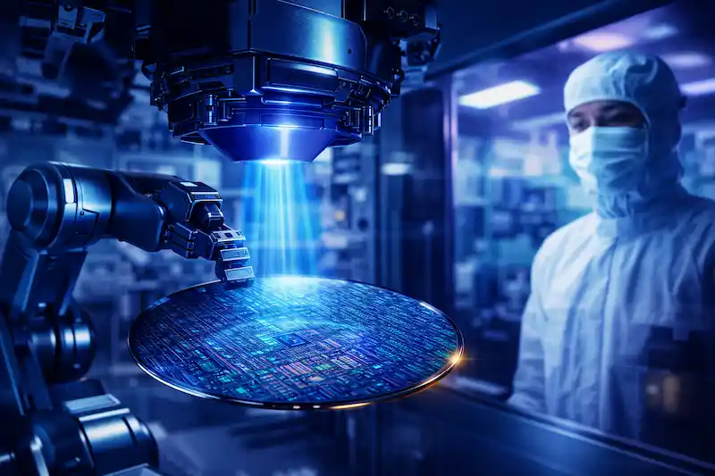
The Pre-Requisite: The Cleanroom Environment
Before we dive into the manufacturing steps, it is crucial to understand where this happens. Chips are manufactured in massive, specialized facilities called Fabs (Fabrication Plants). Inside a Fab is the “Cleanroom.”
Because the transistors on a modern chip are smaller than a virus, a single speck of dust, a stray skin cell, or a micro-droplet of moisture can ruin an entire circuit. Cleanrooms are strictly rated by how many particles are in the air. A Class 1 cleanroom maintains less than one particle of dust per cubic foot of air. Workers must wear specialized “bunny suits” that cover their entire bodies to prevent human contamination from ruining the highly sensitive wafers.
Step-by-Step Chip Fabrication Process
The journey from sand to a working processor takes about 3 to 4 months and involves hundreds of individual steps. Here is the breakdown of the core phases:
Step 1: Wafer Preparation (From Sand to Silicon)
The journey of a microchip begins with plain sand (silicon dioxide). Silicon is the second most abundant element on Earth, making it an ideal and stable base material.
Purification: The sand is melted and refined to produce Electronic Grade Silicon (EGS), which is 99.9999999% pure (often referred to as “nine nines” purity).
Crystal Growth (The Czochralski Process): A tiny “seed” crystal of silicon is dipped into a vat of molten pure silicon. It is slowly rotated and pulled upwards. The molten silicon crystallizes around the seed, forming a massive, perfectly structured cylindrical ingot.
Slicing the Wafer: This solid silicon cylinder is then sliced into incredibly thin discs using a diamond-edged saw. These discs are called wafers (usually 300mm or 12 inches in diameter).
Polishing: The sliced wafers are mechanically and chemically polished until they are completely flawless and mirror-smooth. Any microscopic bump could ruin the microscopic circuits.
Step 2: Deposition
Now that we have a blank canvas (the wafer), we need to start building layers. The first step in creating the actual circuitry is adding thin layers of various materials to the wafer’s surface.
Insulating Layers: Materials like silicon dioxide are deposited to prevent electrical current from leaking where it shouldn’t.
Conducting Layers: Metals are deposited to allow electricity to flow between components. These layers are applied using highly controlled techniques like Chemical Vapor Deposition (CVD), where gases react to form a solid microscopic film on the wafer.
Step 3: Photoresist Coating
To print a complex circuit design onto the wafer, it must be made sensitive to light. The wafer is placed in a machine where it spins at high speeds. While spinning, a light-sensitive liquid chemical called Photoresist is poured onto the center. The centrifugal force spreads the photoresist into an incredibly thin, even layer across the entire wafer.
Step 4: Photolithography (The Magic of Light)
This is arguably the most critical and complex step in the entire chip fabrication process. Photolithography is essentially a highly advanced version of film photography at an atomic scale.
The Mask: Engineers design the chip’s circuitry on computers. This design is printed onto a glass plate called a “photomask” or “reticle.”
Exposure: An extremely precise laser beam (often Extreme Ultraviolet or EUV light in the most advanced chips) shines through the photomask.
Lenses: Because the design on the mask is much larger than the final chip, the light passes through a series of specialized mirrors and lenses that shrink the pattern down to a microscopic size before it hits the wafer.
Printing: The light hits the photoresist on the wafer. The areas exposed to light undergo a chemical change, making them soluble, while the unexposed areas remain hardened.
Step 5: Etching
Once the pattern is printed in the photoresist, the wafer moves to the etching phase. The goal here is to remove the underlying material only where the photoresist was softened by the light.
Dry Etching (Plasma Etching): Modern fabs primarily use dry etching. It uses ionized gases (plasma) to precisely blast away the exposed material at a microscopic level. Once the etching is complete, the remaining hardened photoresist is chemically washed away, leaving behind a 3D pattern etched directly into the silicon or the deposited layers.
Step 6: Doping (Ion Implantation)
Pure silicon is actually a poor conductor of electricity. To make it a semiconductor (a material that can act as both a conductor and an insulator to control the flow of electricity), we must introduce impurities. This process is called Doping.
The wafer is bombarded with beams of high-energy ions (like boron or phosphorus). These ions embed themselves into the areas of the silicon that were exposed during the etching process. By carefully arranging positive (P-type) and negative (N-type) regions, engineers create the actual Transistors—the tiny gates that control electrical current.
Step 7: Interconnects (Back-End-Of-Line – BEOL)
At this point, billions of microscopic transistors have been successfully created on the wafer (this phase is called Front-End-Of-Line or FEOL). However, they are isolated. To make them work together as a processor, they must be wired together.
Microscopic trenches are etched into a dielectric (insulating) layer above the transistors. Copper is then deposited into these trenches to create microscopic wires. A modern chip might have anywhere from 10 to 30 layers of these complex copper wiring networks stacked on top of each other, resembling an incredibly dense, multi-level microscopic city highway system.
Step 8: Wafer Testing (Die Sort)
Once all layers are complete, the wafer contains hundreds of identical individual chips, known as “dies.” Before they are cut apart, they undergo rigorous testing. A machine called a “wafer prober” places microscopic needles onto the contact pads of each individual die. It runs electrical signals through the chip to see if it responds correctly. Defective dies are marked so they can be discarded later.
Step 9: Dicing
The completed, tested wafer is mounted on a sticky blue tape. A highly precise automated saw with a diamond blade—or a targeted laser—cuts the wafer into a grid, separating all the individual dies.
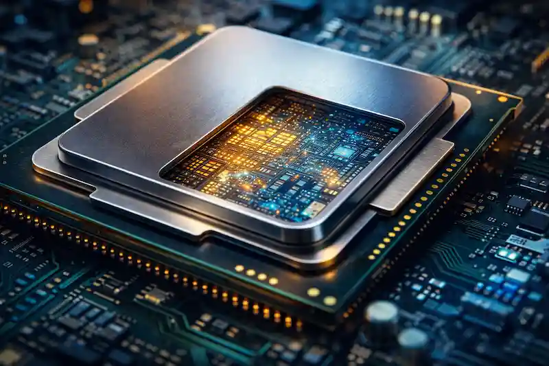
Step 10: Packaging
A bare silicon die is incredibly fragile. It needs a housing to protect it and connect it to a motherboard.
Mounting: The working die is placed onto a substrate (a small circuit board).
Bonding: Microscopic gold or copper wires (or tiny solder bumps) connect the pads on the silicon die to the pins on the substrate.
Encapsulation: A heat-spreader (usually a metallic lid) is placed over the die, and it is sealed with a protective resin. This protects the delicate silicon from physical damage and moisture, while also helping to dissipate the intense heat the chip will generate when running.
Step 11: Final Testing and Binning
The packaged chip goes through one last round of extreme testing under high temperatures and heavy software workloads. This step also involves “Binning.” Chips that perform flawlessly at maximum speeds are sold as premium, top-tier processors. Chips that work perfectly but maybe get a little too hot at max speeds are slightly down-clocked and sold as more affordable, mid-tier processors.
The Future of Chip Fabrication and Artificial Intelligence
For decades, the semiconductor industry has been guided by Moore’s Law, which predicted that the number of transistors on a chip would double roughly every two years. To achieve this, companies like TSMC, Intel, and Samsung have shrunk transistors to mind-boggling sizes—currently reaching 3-nanometer (nm) and 2nm nodes.
These advanced fabrication nodes are the primary driving force behind the global Artificial Intelligence boom. The massive computing power required to train Large Language Models (LLMs) and run complex generative AI tasks is entirely dependent on cutting-edge semiconductor manufacturing. Without these microscopic advancements in hardware, the AI software revolution would simply not be possible.
This hardware evolution is paving the way for massive technological shifts worldwide, much like the ones discussed in our detailed analysis of [Bharat Bodhan AI: A Transformative Revolution for Digital India]. As fabrication technology moves towards new 3D transistor architectures (like GAAFETs) and new materials beyond silicon, the capabilities of AI will only continue to expand.
Conclusion
The chip fabrication process is the unsung hero of the modern age. It takes a raw material found on beaches and turns it into the engines that drive artificial intelligence, space exploration, global communication, and medical breakthroughs.
Taking months to complete and involving hundreds of distinct, nanometer-precise steps, semiconductor manufacturing remains the most advanced production process in human history. Understanding how these chips are made gives us a profound appreciation for the digital tools and devices we rely on every single day.
Frequently Asked Questions (FAQs)
1. How long does it take to manufacture a single microchip? From a raw silicon wafer to a completed, packaged chip, the entire fabrication process usually takes about 3 to 4 months. The wafer must go through hundreds of individual steps, often repeating the lithography, etching, and deposition cycles over and over.
2. Which companies are the biggest chip manufacturers? The companies that physically manufacture the chips are called “Foundries.” The largest and most advanced in the world is TSMC (Taiwan Semiconductor Manufacturing Company), followed by companies like Samsung and Intel. Companies like Apple, AMD, and Nvidia design their chips but usually hire TSMC to manufacture them.
3. What does “3nm” or “5nm” mean in chip making? Historically, this referred to the physical length of the transistor gate. Today, it is more of an industry marketing term used to represent a new “generation” or “node” of manufacturing technology. Generally, a smaller nanometer (nm) number means smaller transistors, allowing more to fit on a chip for higher performance and lower power consumption.
4. Why is chip manufacturing so expensive? The equipment required is incredibly advanced. A single ASML EUV lithography machine, used to print the smallest circuits using extreme ultraviolet light, costs over $150 million. Building a complete, state-of-the-art Fab can cost upwards of $20 Billion due to the extreme cleanroom requirements, advanced robotics, and precision tools needed.
Explore More on MasterWebTool:


